Stress and Strain Engineering at Nanoscale in Semiconductor Devices 1st Edition by Chinmay K. Maiti 0367519291 9780367519292
Original price was: $50.00.$25.00Current price is: $25.00.
Stress and Strain Engineering at Nanoscale in Semiconductor Devices 1st Edition Chinmay K. Maiti – Ebook Instant Download/Delivery ISBN(s): 9780367519292,0367519291

Product details:
• ISBN 10: 0367519291
• ISBN 13: 9780367519292
• Author:
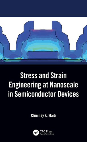
Anticipating a limit to the continuous miniaturization (More-Moore), intense research efforts are being made to co-integrate various functionalities (More-than-Moore) in a single chip. Currently, strain engineering is the main technique used to enhance the performance of advanced semiconductor devices. Written from an engineering applications standpoint, this book encompasses broad areas of semiconductor devices involving the design, simulation, and analysis of Si, heterostructure silicongermanium (SiGe), and III-N compound semiconductor devices. The book provides the background and physical insight needed to understand the new and future developments in the technology CAD (TCAD) design at the nanoscale.
Table contents:
Chapter 1: Introduction
Chapter 2: Simulation Environment
Chapter 3: Stress Generation Techniques in CMOS Technology
Chapter 4: Electronic Properties of Engineered Substrates
Chapter 5: Bulk-Si FinFETs
Chapter 6: Strain-Engineered FinFETs at NanoScale
Chapter 7: Technology CAD of III-Nitride Based Devices
Chapter 8: Strain-Engineered SiGe Channel TFTs for Flexible Electr
People also search:
stress strain definition engineering
what is engineering stress and strain
stress definition engineering
stress vs strain geology
stress analysis engineer
stress analysis engineer jobs
You may also like…
Mathematics - Mathematical Statistics
Multivariate Statistical Modeling in Engineering and Management 1st Edition Jhareswar Maiti
Technique - Electronics
Transport in Semiconductor Mesoscopic Devices 2nd Edition by David K. Ferry 9780750331395 0750331399

Uncategorized
De Stress at Work Understanding and Combatting Chronic Stress 1st Edition Simon L Dolan

Uncategorized
Physics - Quantum Physics
Introduction to Semiconductor Physics and Devices Mykhaylo Evstigneev
Uncategorized
Solutions Manual for Semiconductor Physics and Devices Basic Principles 4th Edition D A Neamen

Science (General)
Semiconductor Devices and Technologies for Future Ultra Low Power Electronics 1st Edition
Uncategorized